欢迎光临!1kic网专注于为电子元器件行业提供免费及更实惠的芯片ic交易网站。
DRV8846 双通道 H 桥步进电机驱动器
DRV8846 Dual H-Bridge Stepper Motor Driver
TI公司的DRV8846是高度集成的步进马达驱动器,包括两个H桥和微步进分度器,工作电压4-18V,驱动电流高达1A,主要用在打印机,扫描仪,视频安全摄像机和投映仪.本文介绍了DRV8846主要特性,功能框图,应用电路以及评估板主要特性,电路图和材料清单,以及3D打印机控制器(12V)主要特性,电路图和材料清单.
• Projectors

图1. DRV8846功能框图
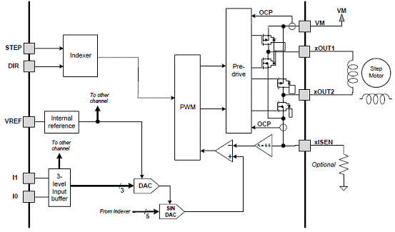
图2. DRV8846 PWM马达驱动器电路图

图3. DRV8846 典型应用电路图
评估板
The DRV8846 customer EVM is a platform revolving around the DRV8846, a low voltage dual H-bridge driver and highly configurable power stage. This device has been optimized to drive a single bipolar stepper with up to 32 degrees of internally generated microstepping.
The EVM houses an MSP430 microcontroller and a USB interface chip. The USB chip allows for serial communications from a PC computer where a Microsoft® Windows® application is used to schedule serial commands. These commands can be used to control each of the device’s signals, and drive the stepper motor by issuing the step commands at the desired rate.
The microcontroller firmware operates using internal index mode.
This user’s guide details the operation of the EVM, as well as the hardware configurability of the evaluation module.

图4.评估板PCB外形图

图5.评估板连接图
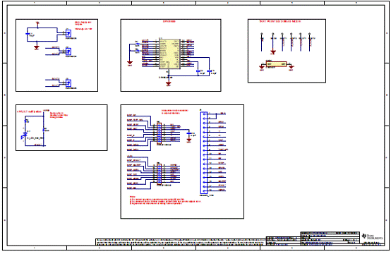
图6.评估板电路图(1)
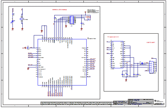
图7.评估板电路图(2)
评估板材料清单:

3D打印机控制器(12V)
This design is a complete system for controlling 3-axis, single extruder-based 3D printers. The system is managed by the MSP430F5529 LaunchPad and utilizes the DRV8846 for precision stepper motor control. The CSD18534Q5A is used as a low-side switch for the hot bed heater, extruder heater, and cooling fan. The DRV5033 Hall Sensor acts as a contactless limit switch.
3D打印机控制器(12V)主要特性:
Complete 3D printer controller with MCU, stepper drivers, heater outputs, sensor inputs, and SD card slot.
Precise stepper motor current regulation using DRV8846 adaptive decay
Hall sensor limit switches are immune to contaminants and never wear out
High-current heater outputs from the CSD18534Q5A with low 7.8 mΩ Rds(ON)
Powered from a single 12V supply
System has been fully tested and proven

图8.3D打印机TIDA-00405外形图

图9.3D打印机TIDA-00405电路图(1)

图10.3D打印机TIDA-00405电路图(2)

图11.3D打印机TIDA-00405电路图(3)
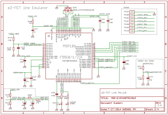
图12.3D打印机TIDA-00405电路图(4)
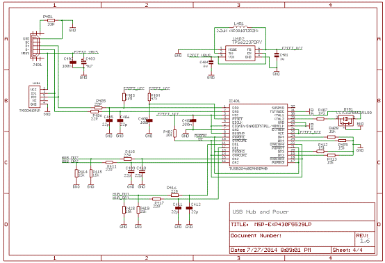
图13.3D打印机TIDA-00405电路图(5)
3D打印机TIDA-00405系统材料清单:


参考资料:
The DRV8846 is an integrated motor driver solution for bipolar stepper motors. The device integrates 2 H-bridges that use NMOS low-side drivers and PMOS high-side drivers, current sense regulation circuitry, and a microstepping indexer. The DRV8846 can be powered with a supply range between 4 to 18 V and is capable of providing an output current to 1.4-A full scale or 1-A rms.
A simple STEP/DIR interface allows easy interfacing to the controller circuit. The internal indexer is able to execute high-accuracy microstepping without requiring the processor to control the current level.
The PWM off-time, tOFF can be adjusted to 10, 20, or 30 μs.
The DRV8846 has an adaptive decay feature that automatically adjusts the decay setting to minimize current ripple while still reacting quickly to step changes. This feature allows the DRV8846 to quickly be integrated into a system.
A torque DAC feature allows the controller to scale the output current without needing to scale the analog reference voltage input VREF. The torque DAC is accessed using digital input pins. This allows the controller to save power by decreasing the current consumption when not required.
A low-power sleep mode is included, which allows the system to save power when not driving the motor.

DRV8846 contains two identical H-bridge motor drivers with current-control PWM circuitry. Figure 6 shows a block diagram of the circuitry.
 Figure 6. PWM Motor Driver Circuitry
To allow a simple step and direction interface to control stepper motors, the DRV8846 contains a microstepping indexer. The indexer controls the state of the H-bridges automatically. When the correct transition is applied at the STEP input, the indexer moves to the next step, according to the direction set by the DIR pin. In 1/8, 1/16, and 1/32 step modes, both the rising and falling edges of the STEP input may be used to advance the indexer, depending on the M0 / M1 setting.
The nENBL pin disables the output stage in indexer mode. When nENBL = 0, the indexer inputs are still active and respond to the STEP and DIR input pins; only the output stage is disabled.
The indexer logic in the DRV8846 allows a number of different stepping configurations. The M0 and M1 pins configure the stepping format (see Table 2).
| M1 | M0 | STEP MODE |
|---|---|---|
| 0 | 0 | Full step (2-phase excitation), rising-edge only |
| 0 | Z | 1/2 step (1-2 phase excitation), rising-edge only |
| 0 | 1 | 1/4 step (W1-2 phase excitation), rising-edge only |
| Z | 0 | 8 microsteps/step, rising-edge only |
| Z | Z | 8 microsteps/step, rising and falling edges |
| Z | 1 | 16 microsteps/step, rising-edge only |
| 1 | 0 | 16 microsteps/step, rising and falling edges |
| 1 | Z | 32 microsteps/step, rising-edge only |
| 1 | 1 | 32 microsteps/step, rising and falling edges |
Note that the M0 and M1 pins are tri-level inputs. These pins can be driven logic low, logic high, or high-impedance (Z), like the I0 and I1 pins described previously.
For 1/8, 1/16, and 1/32-step modes, selections are available to advance the indexer only on the rising edge of the STEP input, or on both the rising and falling edges.
The step mode may be changed on-the-fly while the motor is moving. The indexer advances to the next valid state for the new M0 / M1 setting at the next rising edge of STEP.
The home state is 45°. The indexer enters the home state after power-up, after exiting UVLO, or after exiting sleep mode (see the yellow-shaded cells in Table 3 also indicated with a table note).
Table 3 shows the relative current and step directions for different step mode settings. At each rising edge of the STEP input, the indexer travels to the next state in the table. The direction is shown with the DIR pin high; if the DIR pin is low, the sequence is reversed. Positive current is defined as xOUT1 = positive with respect to xOUT2.
| 1/32 STEP | 1/16 STEP | 1/8 STEP | 1/4 STEP | 1/2 STEP | FULL STEP 70% | WINDING CURRENT A | WINDING CURRENT B | ELECTRICAL ANGLE |
|---|---|---|---|---|---|---|---|---|
| 1 | 1 | 1 | 1 | 1 | 100% | 0% | 0 | |
| 2 | 100% | 5% | 3 | |||||
| 3 | 2 | 100% | 10% | 6 | ||||
| 4 | 99% | 15% | 8 | |||||
| 5 | 3 | 2 | 98% | 20% | 11 | |||
| 6 | 97% | 24% | 14 | |||||
| 7 | 4 | 96% | 29% | 17 | ||||
| 8 | 94% | 34% | 20 | |||||
| 9 | 5 | 3 | 2 | 92% | 38% | 23 | ||
| 10 | 90% | 43% | 25 | |||||
| 11 | 6 | 88% | 47% | 28 | ||||
| 12 | 86% | 51% | 31 | |||||
| 13 | 7 | 4 | 83% | 56% | 34 | |||
| 14 | 80% | 60% | 37 | |||||
| 15 | 8 | 77% | 63% | 39 | ||||
| 16 | 74% | 67% | 42 | |||||
| 17(1) | 9(1) | 5(1) | 3(1) | 2(1) | 1(1) | 71% | 71% | 45 |
| 18 | 67% | 74% | 48 | |||||
| 19 | 10 | 63% | 77% | 51 | ||||
| 20 | 60% | 80% | 53 | |||||
| 21 | 11 | 6 | 56% | 83% | 56 | |||
| 22 | 51% | 86% | 59 | |||||
| 23 | 12 | 47% | 88% | 62 | ||||
| 24 | 43% | 90% | 65 | |||||
| 25 | 13 | 7 | 4 | 38% | 92% | 68 | ||
| 26 | 34% | 94% | 70 | |||||
| 27 | 14 | 29% | 96% | 73 | ||||
| 28 | 24% | 97% | 76 | |||||
| 29 | 15 | 8 | 20% | 98% | 79 | |||
| 30 | 15% | 99% | 82 | |||||
| 31 | 16 | 10% | 100% | 84 | ||||
| 32 | 5% | 100% | 87 | |||||
| 33 | 17 | 9 | 5 | 3 | 0% | 100% | 90 | |
| 34 | –5% | 100% | 93 | |||||
| 35 | 18 | –10% | 100% | 96 | ||||
| 36 | –15% | 99% | 98 | |||||
| 37 | 19 | 10 | –20% | 98% | 101 | |||
| 38 | –24% | 97% | 104 | |||||
| 39 | 20 | –29% | 96% | 107 | ||||
| 40 | –34% | 94% | 110 | |||||
| 41 | 21 | 11 | 6 | –38% | 92% | 113 | ||
| 42 | –43% | 90% | 115 | |||||
| 43 | 22 | –47% | 88% | 118 | ||||
| 44 | –51% | 86% | 121 | |||||
| 45 | 23 | 12 | –56% | 83% | 124 | |||
| 46 | –60% | 80% | 127 | |||||
| 47 | 24 | –63% | 77% | 129 | ||||
| 48 | –67% | 74% | 132 | |||||
| 49 | 25 | 13 | 7 | 4 | 2 | –71% | 71% | 135 |
| 50 | –74% | 67% | 138 | |||||
| 51 | 26 | –77% | 63% | 141 | ||||
| 52 | –80% | 60% | 143 | |||||
| 53 | 27 | 14 | –83% | 56% | 146 | |||
| 54 | –86% | 51% | 149 | |||||
| 55 | 28 | –88% | 47% | 152 | ||||
| 56 | –90% | 43% | 155 | |||||
| 57 | 29 | 15 | 8 | –92% | 38% | 158 | ||
| 58 | –94% | 34% | 160 | |||||
| 59 | 30 | –96% | 29% | 163 | ||||
| 60 | –97% | 24% | 166 | |||||
| 61 | 31 | 16 | –98% | 20% | 169 | |||
| 62 | –99% | 15% | 172 | |||||
| 63 | 32 | –100% | 10% | 174 | ||||
| 64 | –100% | 5% | 177 | |||||
| 65 | 33 | 17 | 9 | 5 | –100% | 0% | 180 | |
| 66 | –100% | –5% | 183 | |||||
| 67 | 34 | –100% | –10% | 186 | ||||
| 68 | –99% | –15% | 188 | |||||
| 69 | 35 | 18 | –98% | –20% | 191 | |||
| 70 | –97% | –24% | 194 | |||||
| 71 | 36 | –96% | –29% | 197 | ||||
| 72 | –94% | –34% | 200 | |||||
| 73 | 37 | 19 | 10 | –92% | –38% | 203 | ||
| 74 | –90% | –43% | 205 | |||||
| 75 | 38 | –88% | –47% | 208 | ||||
| 76 | –86% | –51% | 211 | |||||
| 77 | 39 | 20 | –83% | –56% | 214 | |||
| 78 | –80% | –60% | 217 | |||||
| 79 | 40 | –77% | –63% | 219 | ||||
| 80 | –74% | –67% | 222 | |||||
| 81 | 41 | 21 | 11 | 6 | 3 | –71% | –71% | 225 |
| 82 | –67% | –74% | 228 | |||||
| 83 | 42 | –63% | –77% | 231 | ||||
| 84 | –60% | –80% | 233 | |||||
| 85 | 43 | 22 | –56% | –83% | 236 | |||
| 86 | –51% | –86% | 239 | |||||
| 87 | 44 | –47% | –88% | 242 | ||||
| 88 | –43% | –90% | 245 | |||||
| 89 | 45 | 23 | 12 | –38% | –92% | 248 | ||
| 90 | –34% | –94% | 250 | |||||
| 91 | 46 | –29% | –96% | 253 | ||||
| 92 | –24% | –97% | 256 | |||||
| 93 | 47 | 24 | –20% | –98% | 259 | |||
| 94 | –15% | –99% | 262 | |||||
| 95 | 48 | –10% | –100% | 264 | ||||
| 96 | –5% | –100% | 267 | |||||
| 97 | 49 | 25 | 13 | 7 | 0% | –100% | 270 | |
| 98 | 5% | –100% | 273 | |||||
| 99 | 50 | 10% | –100% | 276 | ||||
| 100 | 15% | –99% | 278 | |||||
| 101 | 51 | 26 | 20% | –98% | 281 | |||
| 102 | 24% | –97% | 284 | |||||
| 103 | 52 | 29% | –96% | 287 | ||||
| 104 | 34% | –94% | 290 | |||||
| 105 | 53 | 27 | 14 | 38% | –92% | 293 | ||
| 106 | 43% | –90% | 295 | |||||
| 107 | 54 | 47% | –88% | 298 | ||||
| 108 | 51% | –86% | 301 | |||||
| 109 | 55 | 28 | 56% | –83% | 304 | |||
| 110 | 60% | –80% | 307 | |||||
| 111 | 56 | 63% | –77% | 309 | ||||
| 112 | 67% | –74% | 312 | |||||
| 113 | 57 | 29 | 15 | 8 | 4 | 71% | –71% | 315 |
| 114 | 74% | –67% | 318 | |||||
| 115 | 58 | 77% | –63% | 321 | ||||
| 116 | 80% | –60% | 323 | |||||
| 117 | 59 | 30 | 83% | –56% | 326 | |||
| 118 | 86% | –51% | 329 | |||||
| 119 | 60 | 88% | –47% | 332 | ||||
| 120 | 90% | –43% | 335 | |||||
| 121 | 61 | 31 | 16 | 92% | –38% | 338 | ||
| 122 | 94% | –34% | 340 | |||||
| 123 | 62 | 96% | –29% | 343 | ||||
| 124 | 97% | –24% | 346 | |||||
| 125 | 63 | 32 | 98% | –20% | 349 | |||
| 126 | 99% | –15% | 352 | |||||
| 127 | 64 | 100% | –10% | 354 | ||||
| 128 | 100% | –5% | 357 |
The current through the motor windings is regulated by an adjustable fixed-off-time PWM current regulation circuit. When an H-bridge is enabled, current rises through the winding at a rate dependent on the DC voltage, inductance of the winding, and the magnitude of the back EMF present. After the current reaches the current chopping threshold, the bridge enters a decay mode for a fixed period of time to decrease the current, which is configurable between 10 to 30 μs through the tri-level input TOFF_SEL. After the time expires, the bridge is re-enabled, starting another PWM cycle.
| TOFF_SEL | TOFF Duration |
|---|---|
| 0 | 20 μs |
| Z | 10 μs |
| 1 | 30 μs |
The PWM chopping current is set by a comparator which compares the voltage across a current sense resistor connected to the xISEN pin, with a reference voltage. The reference voltage can be supplied by an internal reference of 3.3 V (which requires VINT to be connected to VREF), or externally supplied to the VREF pin. The reference voltage is then scaled first by the 3-bit torque DAC, then by the output of a sine lookup table that is applied to a sine-weighted DAC (sine DAC). The voltage is attenuated by a factor of 6.6.
The full-scale (100%) chopping current is calculated as follows:

where
Example: Using VREF is 3.3 V, torque DAC = 100%, and a 500-mΩ sense resistor, the full-scale chopping current is 3.3 V / (6.6 × 500 mΩ) × 100% = 1 A.
The current for both motor windings is scaled depending on the I0 and I1 pins, which drive a 3-bit linear DAC, as inTable 5.
| I1 | I0 | CURRENT SCALING (TORQUE) |
|---|---|---|
| 0 | 0 | 100% |
| 0 | Z | 87.5% |
| 0 | 1 | 75% |
| Z | 0 | 62.5% |
| Z | Z | 50% |
| Z | 1 | 37.5% |
| 1 | 0 | 25% |
| 1 | Z | 12.5% |
| 1 | 1 | 0% (outputs disabled) |
Table 6 gives the xISEN trip voltage at a given DAC code and I[1:0] setting.
| Sine DAC Code | Torque DAC I[1:0] Setting | |||||||
|---|---|---|---|---|---|---|---|---|
| 00 - 100% | 0Z - 87.5% | 01 - 75% | Z0 - 62.5% | ZZ - 50% | Z1 - 37.5% | 10 - 25% | 1Z - 12.5% | |
| 31 | 500 mV | 438 mV | 375 mV | 313 mV | 250 mV | 188 mV | 125 mV | 63 mV |
| 30 | 500 mV | 438 mV | 375 mV | 313 mV | 250 mV | 188 mV | 125 mV | 63 mV |
| 29 | 495 mV | 433 mV | 371 mV | 309 mV | 248 mV | 186 mV | 124 mV | 62 mV |
| 28 | 490 mV | 429 mV | 368 mV | 306 mV | 245 mV | 184 mV | 123 mV | 61 mV |
| 27 | 485 mV | 424 mV | 364 mV | 303 mV | 243 mV | 182 mV | 121 mV | 61 mV |
| 26 | 480 mV | 420 mV | 360 mV | 300 mV | 240 mV | 180 mV | 120 mV | 60 mV |
| 25 | 470 mV | 411 mV | 353 mV | 294 mV | 235 mV | 176 mV | 118 mV | 59 mV |
| 24 | 460 mV | 403 mV | 345 mV | 288 mV | 230 mV | 173 mV | 115 mV | 58 mV |
| 23 | 450 mV | 394 mV | 338 mV | 281 mV | 225 mV | 169 mV | 113 mV | 56 mV |
| 22 | 440 mV | 385 mV | 330 mV | 275 mV | 220 mV | 165 mV | 110 mV | 55 mV |
| 21 | 430 mV | 376 mV | 323 mV | 269 mV | 215 mV | 161 mV | 108 mV | 54 mV |
| 20 | 415 mV | 363 mV | 311 mV | 259 mV | 208 mV | 156 mV | 104 mV | 52 mV |
| 19 | 400 mV | 350 mV | 300 mV | 250 mV | 200 mV | 150 mV | 100 mV | 50 mV |
| 18 | 385 mV | 337 mV | 289 mV | 241 mV | 193 mV | 144 mV | 96 mV | 48 mV |
| 17 | 370 mV | 324 mV | 278 mV | 231 mV | 185 mV | 139 mV | 93 mV | 46 mV |
| 16 | 355 mV | 311 mV | 266 mV | 222 mV | 178 mV | 133 mV | 89 mV | 44 mV |
| 15 | 335 mV | 293 mV | 251 mV | 209 mV | 168 mV | 126 mV | 84 mV | 42 mV |
| 14 | 315 mV | 276 mV | 236 mV | 197 mV | 158 mV | 118 mV | 79 mV | 39 mV |
| 13 | 300 mV | 263 mV | 225 mV | 188 mV | 150 mV | 113 mV | 75 mV | 38 mV |
| 12 | 280 mV | 245 mV | 210 mV | 175 mV | 140 mV | 105 mV | 70 mV | 35 mV |
| 11 | 255 mV | 223 mV | 191 mV | 159 mV | 128 mV | 96 mV | 64 mV | 32 mV |
| 10 | 235 mV | 206 mV | 176 mV | 147 mV | 118 mV | 88 mV | 59 mV | 29 mV |
| 9 | 215 mV | 188 mV | 161 mV | 134 mV | 108 mV | 81 mV | 54 mV | 27 mV |
| 8 | 190 mV | 166 mV | 143 mV | 119 mV | 95 mV | 71 mV | 48 mV | 24 mV |
| 7 | 170 mV | 149 mV | 128 mV | 106 mV | 85 mV | 64 mV | 43 mV | 21 mV |
| 6 | 145 mV | 127 mV | 109 mV | 91 mV | 73 mV | 54 mV | 36 mV | 18 mV |
| 5 | 120 mV | 105 mV | 90 mV | 75 mV | 60 mV | 45 mV | 30 mV | 15 mV |
| 4 | 100 mV | 88 mV | 75 mV | 63 mV | 50 mV | 38 mV | 25 mV | 13 mV |
| 3 | 75 mV | 66 mV | 56 mV | 47 mV | 38 mV | 28 mV | 19 mV | 9 mV |
| 2 | 50 mV | 44 mV | 38 mV | 31 mV | 25 mV | 19 mV | 13 mV | 6 mV |
| 1 | 25 mV | 22 mV | 19 mV | 16 mV | 13 mV | 9 mV | 6 mV | 3 mV |
| 0 | 0 mV | 0 mV | 0 mV | 0 mV | 0 mV | 0 mV | 0 mV | 0 mV |
After the chopping current threshold is reached, the drive current is interrupted, but due to the inductive nature of the motor, current must continue to flow for some period of time (called recirculation current). To handle this recirculation current, the H-bridge can operate in two different states, fast decay or slow decay (or a mixture of fast and slow decay).
In fast-decay mode, after the PWM chopping current level is reached, the H-bridge reverses state to allow winding current to flow through the opposing FETs. As the winding current approaches 0, the bridge is disabled to prevent any reverse current flow. For fast-decay mode, see number 2 in Figure 7.
In slow-decay mode, winding current is recirculated by enabling both of the low-side FETs in the bridge. For slow-decay mode, see number 3 in Figure 7.
 Figure 7. Decay Modes
The DRV8846 supports fast, slow, mixed, and adaptive decay modes. With stepper motors, the decay mode is chosen for a given stepper motor and operating conditions to minimize mechanical noise and vibration.
In mixed decay mode, the current recirculation begins as fast decay, but at a fixed period of time (determined by the state of the DEC1 and DEC0 pins shown in Table 7) the current recirculation switches to slow decay mode for the remainder of the fixed PWM period. Note that the DEC1 and DEC0 pins are tri-level inputs; these pins can be driven logic low, logic high, or high-impedance (Z).
Figure 8 shows the current waveforms in slow, fast, and 25% and 1 tBLANK mixed decay modes.
 Figure 8. Decay Behavior
| DEC1 | DEC0 | Decay Mode (Increasing Current) | Decay Mode (Decreasing Current) |
|---|---|---|---|
| 0 | 0 | Slow decay | Slow decay |
| 0 | Z | Slow decay | Mixed decay: 25% fast |
| 0 | 1 | Slow decay | Mixed decay: 1 tBLANK |
| Z | 0 | Mixed decay: 1 tBLANK | Mixed decay: 1 tBLANK |
| Z | Z | Mixed decay: 50% fast | Mixed decay: 50% fast |
| Z | 1 | Mixed decay: 25% fast | Mixed decay: 25% fast |
| 1 | 0 | Slow decay | Mixed decay: 50% fast |
| 1 | Z | Slow decay | Mixed decay: 12.5% fast |
| 1 | 1 | Slow decay | Fast decay |
Figure 9 shows increasing and decreasing current. When current is decreasing, the decay mode used is fast, slow, or mixed as commanded by the DEC1 and DEC0 pins. Three DEC pin selections allow for mixed decay during increasing current.
 Figure 9. Increasing and Decreasing Current
Adaptive decay mode simplifies the decay mode selection by dynamically changing to adjust for current level, step change, supply variation, BEMF, and load. To enable adaptive decay mode, pull the ADEC pin to logic high and pull DEC0 and DEC1 pins to logic high. The state of the ADEC pin is only evaluated when exiting sleep mode.
Adaptive decay adjusts the time spent in fast decay to minimize current ripple and quickly adjust to current-step changes. If the drive time is longer than the minimum (tBLANK), in order to reach the current trip point, the decay mode applied is slow decay (see Figure 10).
 Figure 10. Adaptive Decay – Slow Decay Operation
When the minimum drive time (tBLANK) provides more current than the regulation point, fast decay of 1- tBLANK is applied. If the second drive period also provides more current than the regulation point, fast decay of 2 tBLANK is applied. If a third (or more) consecutive period provides more current than the regulation point, fast decay using 25% of tOFF time is applied. When the minimum drive time is insufficient to reach the current regulation level, slow decay is applied until the current exceeds the current reference level (see Figure 11).
 Figure 11. Adaptive Decay – Mixed Decay Operation
Figure 12 shows a case for adaptive decay where a step occurs. The system starts with 1 tBLANK of fast decay and works up to 25% of tOFF time for fast decay until the current is regulated again.
 Figure 12. Adaptive Decay – Step Operation
After the current is enabled in an H-bridge, the voltage on the xISEN pin is ignored for a period of time before enabling the current sense circuitry. Note that the blanking time also sets the minimum drive time of the PWM.
The time, tBLANK, is determined by the sine DAC code and the torque DAC setting. The timing information for tBLANK is given in Table 8.
| Sine DAC Code | Torque DAC I[1:0] Setting | |||||||
|---|---|---|---|---|---|---|---|---|
| 00 - 100% | 0Z - 87.5% | 01 - 75% | Z0 - 62.5% | ZZ - 50% | Z1 - 37.5% | 10 - 25% | 1Z - 12.5% | |
| 31 | 1.80 μs | 1.80 μs | 1.50 μs | 1.50 μs | 1.50 μs | 1.20 μs | 1.20 μs | 0.90 μs |
| 30 | 1.80 μs | 1.80 μs | 1.50 μs | 1.50 μs | 1.50 μs | 1.20 μs | 1.20 μs | 0.90 μs |
| 29 | 1.80 μs | 1.80 μs | 1.50 μs | 1.50 μs | 1.50 μs | 1.20 μs | 1.20 μs | 0.90 μs |
| 28 | 1.80 μs | 1.80 μs | 1.50 μs | 1.50 μs | 1.50 μs | 1.20 μs | 1.20 μs | 0.90 μs |
| 27 | 1.80 μs | 1.80 μs | 1.50 μs | 1.50 μs | 1.50 μs | 1.20 μs | 1.20 μs | 0.90 μs |
| 26 | 1.80 μs | 1.80 μs | 1.50 μs | 1.50 μs | 1.50 μs | 1.20 μs | 1.20 μs | 0.90 μs |
| 25 | 1.80 μs | 1.80 μs | 1.50 μs | 1.50 μs | 1.50 μs | 1.20 μs | 1.20 μs | 0.90 μs |
| 24 | 1.80 μs | 1.80 μs | 1.50 μs | 1.50 μs | 1.50 μs | 1.20 μs | 1.20 μs | 0.90 μs |
| 23 | 1.80 μs | 1.80 μs | 1.50 μs | 1.50 μs | 1.50 μs | 1.20 μs | 1.20 μs | 0.90 μs |
| 22 | 1.80 μs | 1.80 μs | 1.50 μs | 1.50 μs | 1.50 μs | 1.20 μs | 1.20 μs | 0.90 μs |
| 21 | 1.80 μs | 1.80 μs | 1.50 μs | 1.50 μs | 1.50 μs | 1.20 μs | 1.20 μs | 0.90 μs |
| 20 | 1.80 μs | 1.80 μs | 1.50 μs | 1.50 μs | 1.50 μs | 1.20 μs | 1.20 μs | 0.90 μs |
| 19 | 1.80 μs | 1.80 μs | 1.50 μs | 1.50 μs | 1.50 μs | 1.20 μs | 1.20 μs | 0.90 μs |
| 18 | 1.80 μs | 1.80 μs | 1.50 μs | 1.50 μs | 1.50 μs | 1.20 μs | 1.20 μs | 0.90 μs |
| 17 | 1.80 μs | 1.80 μs | 1.50 μs | 1.50 μs | 1.50 μs | 1.20 μs | 1.20 μs | 0.90 μs |
| 16 | 1.80 μs | 1.80 μs | 1.50 μs | 1.50 μs | 1.50 μs | 1.20 μs | 1.20 μs | 0.90 μs |
| 15 | 1.50 μs | 1.50 μs | 1.50 μs | 1.20 μs | 1.20 μs | 1.20 μs | 0.90 μs | 0.90 μs |
| 14 | 1.50 μs | 1.50 μs | 1.50 μs | 1.20 μs | 1.20 μs | 1.20 μs | 0.90 μs | 0.90 μs |
| 13 | 1.50 μs | 1.50 μs | 1.50 μs | 1.20 μs | 1.20 μs | 1.20 μs | 0.90 μs | 0.90 μs |
| 12 | 1.50 μs | 1.50 μs | 1.50 μs | 1.20 μs | 1.20 μs | 1.20 μs | 0.90 μs | 0.90 μs |
| 11 | 1.50 μs | 1.50 μs | 1.50 μs | 1.20 μs | 1.20 μs | 1.20 μs | 0.90 μs | 0.90 μs |
| 10 | 1.50 μs | 1.50 μs | 1.50 μs | 1.20 μs | 1.20 μs | 1.20 μs | 0.90 μs | 0.90 μs |
| 9 | 1.50 μs | 1.50 μs | 1.50 μs | 1.20 μs | 1.20 μs | 1.20 μs | 0.90 μs | 0.90 μs |
| 8 | 1.50 μs | 1.50 μs | 1.50 μs | 1.20 μs | 1.20 μs | 1.20 μs | 0.90 μs | 0.90 μs |
| 7 | 1.20 μs | 1.20 μs | 1.20 μs | 0.90 μs | 0.90 μs | 0.90 μs | 0.90 μs | 0.90 μs |
| 6 | 1.20 μs | 1.20 μs | 1.20 μs | 0.90 μs | 0.90 μs | 0.90 μs | 0.90 μs | 0.90 μs |
| 5 | 1.20 μs | 1.20 μs | 1.20 μs | 0.90 μs | 0.90 μs | 0.90 μs | 0.90 μs | 0.90 μs |
| 4 | 1.20 μs | 1.20 μs | 1.20 μs | 0.90 μs | 0.90 μs | 0.90 μs | 0.90 μs | 0.90 μs |
| 3 | 0.90 μs | 0.90 μs | 0.90 μs | 0.90 μs | 0.90 μs | 0.90 μs | 0.90 μs | 0.90 μs |
| 2 | 0.90 μs | 0.90 μs | 0.90 μs | 0.90 μs | 0.90 μs | 0.90 μs | 0.90 μs | 0.90 μs |
| 1 | 0.90 μs | 0.90 μs | 0.90 μs | 0.90 μs | 0.90 μs | 0.90 μs | 0.90 μs | 0.90 μs |
| 0 | 0.90 μs | 0.90 μs | 0.90 μs | 0.90 μs | 0.90 μs | 0.90 μs | 0.90 μs | 0.90 μs |
The DRV8846 is fully protected against undervoltage, overcurrent, and overtemperature events.
An analog current limit circuit on each FET limits the current through the FET by limiting the gate drive. If this analog current limit persists for longer than the OCP deglitch time tOCP, all FETs in the H-bridge are disabled and the nFAULT pin is driven low. The device remains disabled until the retry time, tRETRY, occurs. The OCP is independent for each H-bridge.
Overcurrent conditions are detected independently on both high-side and low-side devices; that is, a short to ground, supply, or across the motor winding all result in an OCP event. Note that OCP does not use the current sense circuitry used for PWM current control, so OCP functions without the presence of the xISEN resistors.
If the die temperature exceeds safe limits, all FETs in the H-bridge are disabled and the nFAULT pin is driven low. After the die temperature falls to a safe level, operation automatically resumes. The nFAULT pin is released after operation has resumed.
If at any time the voltage on the VM pin falls below the UVLO falling threshold voltage, VUVLO, all circuitry in the device is disabled, and all internal logic is reset. Operation resumes when VM rises above the UVLO rising threshold. The nFAULT pin is driven low during an undervoltage condition and is released after operation has resumed.
| Fault | Error Report | H-Bridge | Internal Circuits | Recovery |
|---|---|---|---|---|
| VM UVLO | nFAULT unlatched | Disabled | Shut down | System and fault clears on recovery |
| OCP | nFAULT unlatched | Disabled | Operating | System and fault clears on recovery and motor is driven after time, tRETRY |
| TSD | nFAULT unlatched | Disabled | Operating | System and fault clears on recovery |
1kic网-首个免费IC网-电子元器件ic交易网-芯片集成电路代理商供应商查询